PhD Student
|
Development of monolithic integrated GaAs on Silicon for tandem solar cells I graduated from the Master Material and Nano-Objects Sciences (SMNO) at Sorbonne University and I am now working on the Hello_PV ANR project as a PhD student, under the supervision of Charles Renard and Frederic Hamouda. I’ll attempt to pattern Si surface for the lateral epitaxial growth of AlGaAs/Si photovoltaic tandem cell. |
1) AlGaAs μ-crystals growth on Si
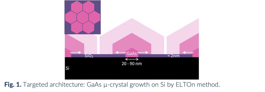
SEEDs team have developed the ELTOn method: Epitaxial Lateral overgrowth on Tunnel Oxide from nano-seed. This involves epitaxial growing GaAs microcrystals from nano-openings (< ø 90 nm) thermally formed in the ultra-thin silicon oxide layer (< 2 nm). This process has demonstrated perfectly epitaxial GaAs microcrystals on silicon without structural defects, with good optoelectronic integration across their entire surface (GaAs/Si and GaAs/SiO2/Si stacking by tunnel effect)
2) Patterning Silicon Surface: The NanoSphere Lithography
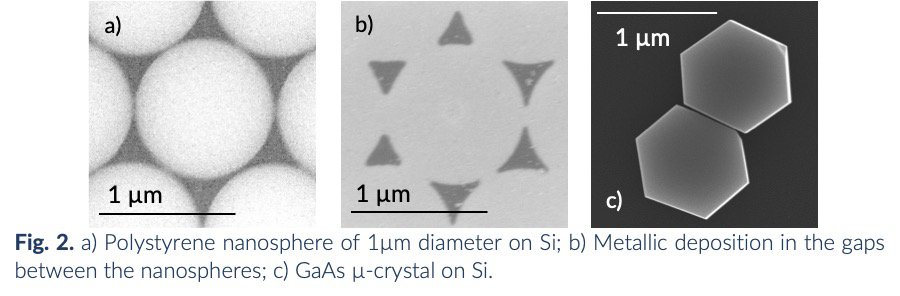
Our current objective is to cover as much silica surface as possible with GaAs to achieve
a quasi-layer. For this purpose, we are developing a quick, reproducible, and cost-effective lithography method based on NanoSphere Lithography (NSL) to localize the growth of µ-crystals
in a hexagonal array. NSL utilizes the self-organization of inexpensive polystyrene beads.
3) Targeted tandem solar cell : AlGaAs/SiO2/Si
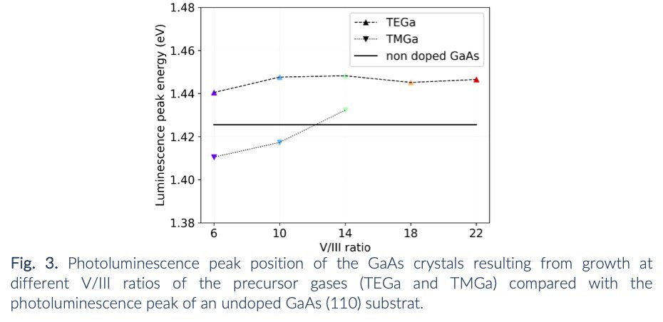
However, previous research used TMGa as a gas precursor for Ga, these resulting crystals showed unintentional P-type doping with carbon, regardless of the V/III ratio [2]. This type of doping is not suitable for the production of a tandem cell demonstrator. To address this issue, it is crucial to be able to control the intentional P and N-type doping of the GaAs crystals, which is essential for creating the PN junction in the tandem cell. Therefore, our focus is on improving dopage control in GaAs integration on Si by using TEGa as the gas precursor for Ga and exploring the incorporation of Aluminum during AlGaAs growth on Si.
Once those methods will be mastered, we will continue to set up the basic bricks for the realization of the PN junction in the crystals of AlGaAs for the realization of a tandem photovoltaic cell on Si.
L. Dentz, Guillaume Chau, G. Hallais, F. Hamouda, James P. Connolly, et al.. DEVELOPMENT OF MONOLITHICALLY INTEGRATED (Al)GaAs ON SILICON FOR TANDEM SOLAR CELLS.
40th European Photovoltaic Solar Energy Conference & Exhibition, Sep 2023, Lisbonne, Portugal. pp.020129-001, 10.4229/EUPVSEC2023/2CV.2.26. hal-04311586

Email address
Office number
C119
Address
C2N
10 Bd Thomas Gobert
91120 Palaiseau FRANCE
Phone number
+33 1 70 27 02 11
Research areas